Timothy Hegarty, Principal Applications Engineer, Isolated and Protection Solutions
Texas Instruments
With the advent of and voracious demand for new handset, tablet and notebook devices with lower profile and smaller form factors, engineers called upon to design solutions that fit into the required footprint dimensions face a particularly arduous task. Furthermore, consumers, while seeking increased functionality and features with their portable devices, place a substantial premium on battery capacity by seeking longer run time between charge cycles. The upshot is that the battery ends up vying for valuable device real estate with the system board, and the PCB area available to portable device designers is even more restricted than at first glance.
The system power demands of these devices are inherently more demanding with new audio, video and processing specifications. For example, smartphone handsets now must seamlessly accommodate multi-mode 3G and 4G wireless communication standards, latest generation wireless local area networks (WLAN), Bluetooth and near field communication (NFC) protocols, touch screen control, and a multi-core, multi-GHz applications processor platform1. Power management of the subsystem blocks becomes a key concern, both in active mode and sleep mode operating regimes. To minimize battery drain, it becomes strategically advantageous to entirely disconnect a particular sub-system block when it is not required and reconnect when needed.
Also, a must have for these devices are connection ports such as USB, stereo headphone mini-jack or proprietary connection that enable a user to hookup various accessories to their device. However, power transfer from a portable device to a downstream accessory needs to be carefully managed to avoid inrush current and mitigate voltage transient events upon connection and disconnection. The accessory typically sends a handshake signal to indicate that it is ready to accept downstream power transfer. Only then should the device’s CPU or system controller authorize current flow. Well-defined overload protection is also mandated to smoothly charge large capacitive loads upon peripheral connection and to reliably manage fault modes that may occur at the load.
Peripheral Connectivity Power Management
There are a number of ways to solve and overcome the peripheral connectivity application challenges referenced above, the most convenient being a load switch IC implementation. This is a series power switch that provides a smart and cost-effective connect/disconnect power distribution function. Specifically, the power switch is implemented using a MOSFET in the power path with its body diode directed such that it cannot pass the load current when the MOSFET is off.
Of course, it is critical to minimize power dissipation to reduce die operating temperature, particularly with small footprint ICs. MOSFET switch on-state resistance has a positive temperature coefficient, which means an increase of junction temperature compounds upon itself to increase even further until a steady state thermal equilibrium is obtained.
What is more, the local ambient and PCB temperatures in high-density PCB layouts can become elevated quickly due to the mutual heating effect inherent with high-power dissipation from immediately adjacent power components, for example: RF PA modules, DC/DC switching regulators, low noise LDO linear regulators, class-D audio amplifiers, display drivers, battery charger ICs, and the like1. These devices can dissipate significant heat, at least on a transient basis. The power and ground planes common to and layered beneath the devices act as heat spreaders throughout the PCB. The thermal properties of the IC package are key to achieving the desired thermal performance. Specifically, low-thermal impedance from junction to soldered pin serves to conduct a large portion of the heat flux through the device pins and utilizes the PCB substrate as a heatsinking element.
Incorporated in the solution with the power MOSFET should be an accurate current sense functional block, a series current sense resistor for example, to protect the input supply in case of large bulk capacitance, over-current or short circuit at the load. Optimal solutions can then avail of a brick-wall current limit characteristic. This leverages an internal current-mode loop that regulates the load current to an essentially constant setpoint as the output voltage falls from its nominal level during an overload event. Moreover, it is important to facilitate smooth entry into and recovery from current limit as substantial inductive circuit parasitics can occur with long connection lines.
Circuit Implementation
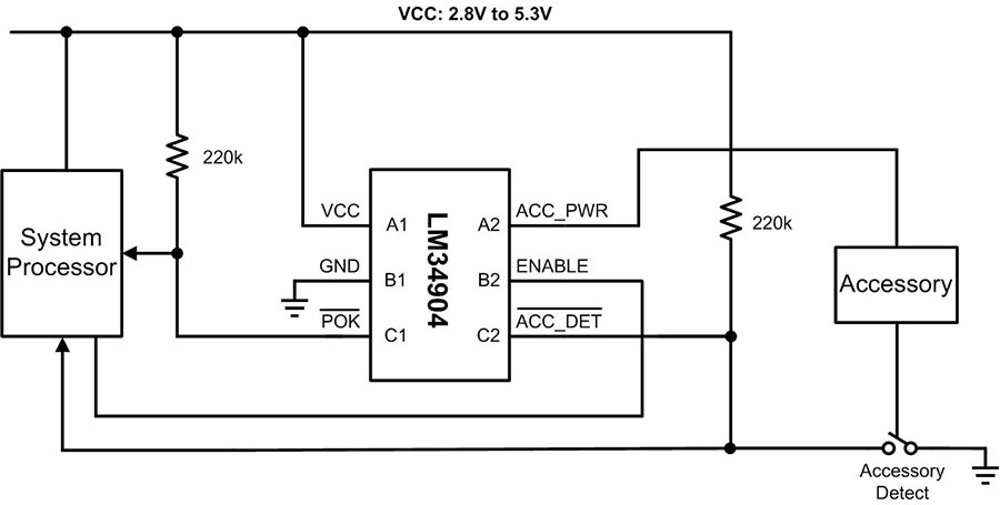
A newly designed smart power switch IC solution in ultra-miniature package combining low on-state resistance and accurate current limit protection2 is now available to address the peripheral connectivity requirements described above. The LM34904 from TI comes in a 1.2-mm by 0.8-mm chip scale package and is rated for 0.5 A continuous current. The schematic in Figure 1 demonstrates how this power switch connects to a device CPU (or microcontroller) and an accessory load.

The power switch IC implementation saves board space, extends battery life and monolithically integrates several safety and protection features. For example, the CPU can check the status of an accessory detect control input and selectively turn on (or off) the MOSFET switch using an enable input. This provides power to the accessory or dynamically conserving power when needed. An open-drain output flag provides switch status to the CPU. Power transfer can also be initiated based on this signal transition.
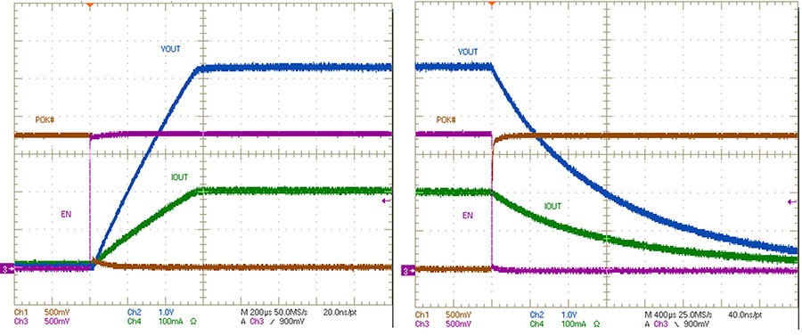
The scope waveforms presented in Figure 2a show the startup behavior when Enable goes high for a 5.3 V supply rail and 47-µF of load capacitance3. Constant current charging results in an approximately linear charging ramp of the output voltage. Figure 2b shows the corresponding shutdown disconnect waveforms.

Conclusion
Understanding the application considerations and challenges associated with connecting peripheral accessories to battery-powered portable devices in an optimal and effective manner is an important task. An appreciation of the design goals and attributes pertaining to peripheral connectivity power management coupled with potential effects from adjacent circuit blocks is provided in the foregoing. Additionally, an implementation using a current-limited smart power switch IC indicative of the primary design requirements such as high-density, efficiency and cost effectiveness, is illustrated to reinforce the key considerations and gain some useful design insight.
References
1. Smartphone Handset system block diagram: http://www.ti.com/smartphonesbd-ca.
2. 500 mA current limited power switch,” Datasheet (SNVS803D), Texas Instruments, 2012.
3. “LM34904 Evaluation Module,” Tim Hegarty, Texas Instruments, July 2012.
Timothy Hegarty is a principal applications engineer in the Power Products Business Unit at Texas Instruments. He received his bachelor’s and master’s degrees in Electrical Engineering from University College Cork, Ireland. Prior to joining Texas Instruments, he worked for National Semiconductor and Artesyn Technologies. His areas of interest are integrated PWM switching regulators and controllers, LDOs, references, hot-swap and ORing system protection and management controllers, renewable energy systems, and system-level simulation of same. He is a member of the IEEE Power Electronics Society.
For more information, please contact Tim at ti_timhegarty@list.ti.com or visit www.ti.com.


